Semiconductor & High-Purity Materials
Trace metals in wafers, process chemicals and ultrapure water.
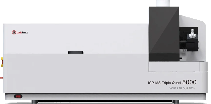
The workflow
Semiconductor analysis is a contamination problem before it is an analytical problem. Every touch point — the acid, the vessel, the autosampler, the laboratory air — sets the floor of the detection limit.
The catalog addresses the whole chain: sub-boiling acid purification, single-chamber digestion, ICP-MS and ICP-MS/MS with collision-reaction cell technology and SEMI S2 safety certification, automated sample introduction for high-throughput fabs, and ultra-clean laboratory design.
What makes it difficult
- Reaching ultra-trace detection limits in high-matrix process chemicals
- Controlling contamination from reagents, vessels and the laboratory environment
- Removing polyatomic interferences without losing sensitivity
- Automating calibration and sample introduction in a production environment
Typical samples
Recommended systems
ICP-MS · TotaLab Automation · Acid Purification · Clean Labs & Furniture · Consumables
Step by step
How the sample moves.
Purify reagents
Sub-boiling distillation produces the low-blank acids that trace analysis depends on.
Acid Purification →Prepare
Single-chamber digestion and automated acid dispensing for wafers, slurries and chemicals.
Microwave Digestion →Analyze
ICP-MS and ICP-MS/MS with collision-reaction cell technology and SEMI S2 certification.
ICP-MS →Automate
TotaLab systems prepare calibration curves, dilute and introduce samples on-line.
TotaLab Automation →Systems
Recommended for Semiconductor & High-Purity Materials.
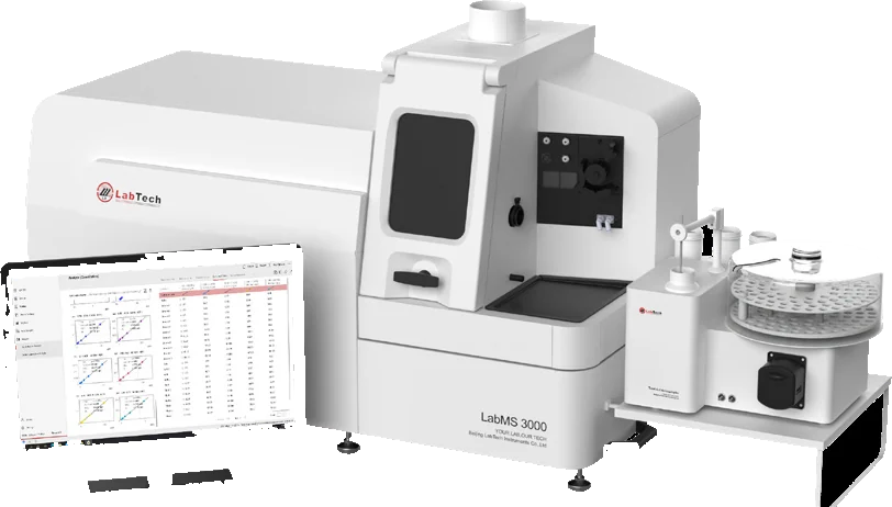
Single-quadrupole and triple-quadrupole trace-element analysis.
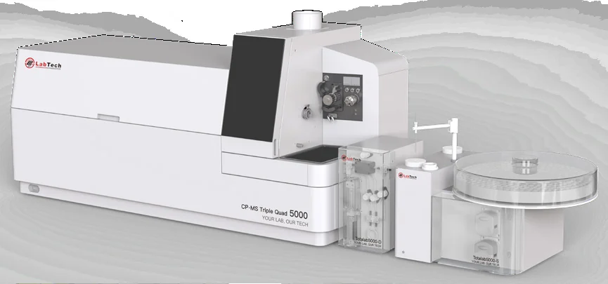
Modular ICP-MS and ICP-OES sample preparation, calibration and introduction.
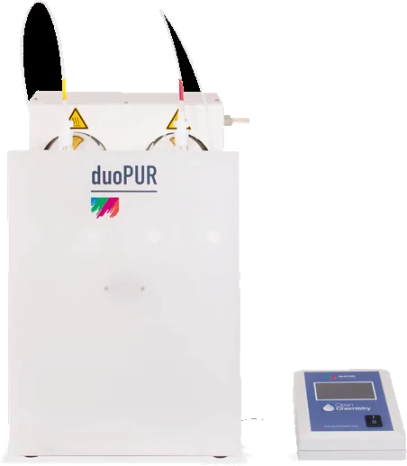
Sub-boiling acid purification and reflux cleaning for ultra-trace blanks.
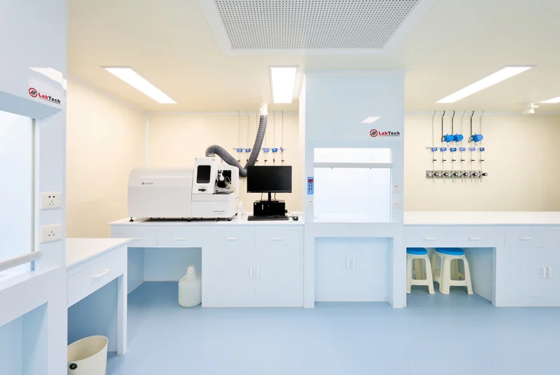
Designed, built, and equipped clean laboratories for trace and isotope analysis.
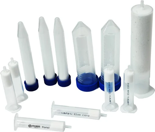
Membrane SPE, sample prep consumables, air monitoring tubes, and analyzer accessories.
Send us the regulation and the limit
We map it to a LabTech configuration and tell you where the catalog stops short of your specification.